(Summary description)Silicon optical technology is simply "light instead of electricity", by integrating a large number of optical devices into a single silicon optical chip to significantly reduce the size of optical modules, simplify the design and production of optical modules.
Silicon optical technology can be combined with integrated circuit technology to ultimately achieve the integration of optical and electrical chips to achieve chip and chip or even chip internal optical interconnection. Silicon optical technology has the outstanding advantages of high connection speed, low power consumption, high speed, and compact structure, which can be said to be the key technology to solve the bottlenecks of power consumption, speed, and volume faced by information networks at present.
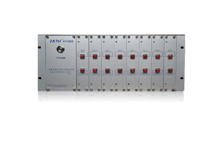
Traditional optical modules use discrete structure, optical chip through a series of passive coupling devices, and optical fiber to achieve alignment coupling, to complete the optical circuit packaging. The entire packaging process requires more material and labor costs, while the packaging and testing process is more complex, the automation rate of the packaging process is low, and the testing requires manual alignment and coupling testing of the optical modules one by one, which results in higher time and labor costs.
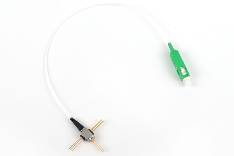
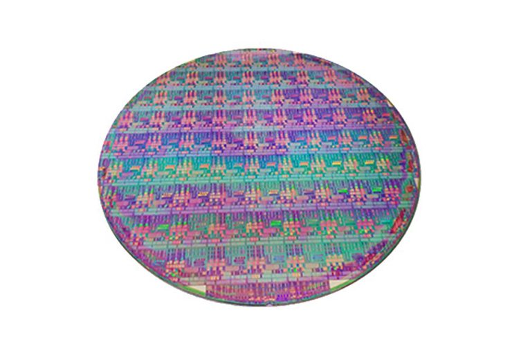
Silicon light using the traditional semiconductor industry is very mature silicon wafer processing process, the use of etching process on a silicon substrate can be quickly processed large-scale waveguide devices, the use of epitaxial growth and other processing processes, the ability to prepare modulators, receivers and other key devices, and ultimately achieve a high degree of integration of modulators, receivers and passive optical devices.
Compared with traditional discrete devices, the traditional process requires the sequential packaging of electrical chips, optical chips, lenses, alignment components, fiber ends and other devices, silicon optical volume significantly reduced, material costs, chip costs, packaging costs are expected to be further optimized, at the same time, silicon optical technology can be tested in bulk through wafer testing and other methods, testing efficiency significantly improved.
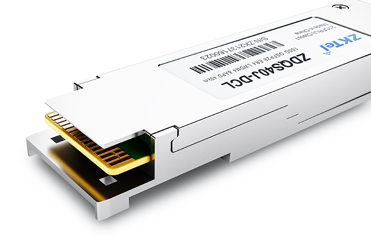
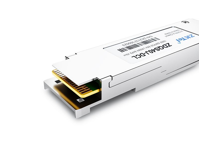
The 100G CWDM4 silicon optical module launched by ZKTel last year is a hot-swappable QSFP28 package with 4-channel full-duplex transceiver and duplex LC optical port; it complies with QSFP28 MSA and CWDM4 MSA standards with the highest rate up to 103.125Gbps; the product is a 100G transmission mode based on single-mode coarse wavelength division multiplexing (CWDM) technology, using 1271nm, 1291nm, 1311nm and 1331nm, the four central wavelengths for optical signal transmission, each band transmission 25G; is both small size, high speed, low power consumption of the new generation of products, can be applied to data center 100G CWDM4 Ethernet, InfiniBand EDR high-performance computing and storage network. At present, the silicon optical module has been certified by several module manufacturers and achieved mass production. Welcome customers who need to discuss cooperation!
(Summary description)Silicon optical technology is simply "light instead of electricity", by integrating a large number of optical devices into a single silicon optical chip to significantly reduce the size of optical modules, simplify the design and production of optical modules.
Silicon optical technology can be combined with integrated circuit technology to ultimately achieve the integration of optical and electrical chips to achieve chip and chip or even chip internal optical interconnection. Silicon optical technology has the outstanding advantages of high connection speed, low power consumption, high speed, and compact structure, which can be said to be the key technology to solve the bottlenecks of power consumption, speed, and volume faced by information networks at present.
Traditional optical modules use discrete structure, optical chip through a series of passive coupling devices, and optical fiber to achieve alignment coupling, to complete the optical circuit packaging. The entire packaging process requires more material and labor costs, while the packaging and testing process is more complex, the automation rate of the packaging process is low, and the testing requires manual alignment and coupling testing of the optical modules one by one, which results in higher time and labor costs.
Silicon light using the traditional semiconductor industry is very mature silicon wafer processing process, the use of etching process on a silicon substrate can be quickly processed large-scale waveguide devices, the use of epitaxial growth and other processing processes, the ability to prepare modulators, receivers and other key devices, and ultimately achieve a high degree of integration of modulators, receivers and passive optical devices.
Compared with traditional discrete devices, the traditional process requires the sequential packaging of electrical chips, optical chips, lenses, alignment components, fiber ends and other devices, silicon optical volume significantly reduced, material costs, chip costs, packaging costs are expected to be further optimized, at the same time, silicon optical technology can be tested in bulk through wafer testing and other methods, testing efficiency significantly improved.
The 100G CWDM4 silicon optical module launched by ZKTel last year is a hot-swappable QSFP28 package with 4-channel full-duplex transceiver and duplex LC optical port; it complies with QSFP28 MSA and CWDM4 MSA standards with the highest rate up to 103.125Gbps; the product is a 100G transmission mode based on single-mode coarse wavelength division multiplexing (CWDM) technology, using 1271nm, 1291nm, 1311nm and 1331nm, the four central wavelengths for optical signal transmission, each band transmission 25G; is both small size, high speed, low power consumption of the new generation of products, can be applied to data center 100G CWDM4 Ethernet, InfiniBand EDR high-performance computing and storage network. At present, the silicon optical module has been certified by several module manufacturers and achieved mass production. Welcome customers who need to discuss cooperation!
- Categories:Tech Support
- Author:
- Origin:
- Time of issue:2023-01-05 14:36
- Views:
Silicon optical technology is simply "light instead of electricity", by integrating a large number of optical devices into a single silicon optical chip to significantly reduce the size of optical modules, simplify the design and production of optical modules.
Silicon optical technology can be combined with integrated circuit technology to ultimately achieve the integration of optical and electrical chips to achieve chip and chip or even chip internal optical interconnection. Silicon optical technology has the outstanding advantages of high connection speed, low power consumption, high speed, and compact structure, which can be said to be the key technology to solve the bottlenecks of power consumption, speed, and volume faced by information networks at present.
Traditional optical modules use discrete structure, optical chip through a series of passive coupling devices, and optical fiber to achieve alignment coupling, to complete the optical circuit packaging. The entire packaging process requires more material and labor costs, while the packaging and testing process is more complex, the automation rate of the packaging process is low, and the testing requires manual alignment and coupling testing of the optical modules one by one, which results in higher time and labor costs.

Silicon light using the traditional semiconductor industry is very mature silicon wafer processing process, the use of etching process on a silicon substrate can be quickly processed large-scale waveguide devices, the use of epitaxial growth and other processing processes, the ability to prepare modulators, receivers and other key devices, and ultimately achieve a high degree of integration of modulators, receivers and passive optical devices.
Compared with traditional discrete devices, the traditional process requires the sequential packaging of electrical chips, optical chips, lenses, alignment components, fiber ends and other devices, silicon optical volume significantly reduced, material costs, chip costs, packaging costs are expected to be further optimized, at the same time, silicon optical technology can be tested in bulk through wafer testing and other methods, testing efficiency significantly improved.
The 100G CWDM4 silicon optical module launched by ZKTel last year is a hot-swappable QSFP28 package with 4-channel full-duplex transceiver and duplex LC optical port; it complies with QSFP28 MSA and CWDM4 MSA standards with the highest rate up to 103.125Gbps; the product is a 100G transmission mode based on single-mode coarse wavelength division multiplexing (CWDM) technology, using 1271nm, 1291nm, 1311nm and 1331nm, the four central wavelengths for optical signal transmission, each band transmission 25G; is both small size, high speed, low power consumption of the new generation of products, can be applied to data center 100G CWDM4 Ethernet, InfiniBand EDR high-performance computing and storage network. At present, the silicon optical module has been certified by several module manufacturers and achieved mass production. Welcome customers who need to discuss cooperation!